How to Troubleshoot a PCB Design 8 Steps with Pictures Circuit Diagram Strong adhesion between the copper traces and the PCB substrate is crucial for the durability and reliability of the board. The Peel Test ensures that the copper traces will not separate from the substrate during manufacturing or operation, preventing electrical failures and extending the lifespan of the PCB. 21. Accelerated Life Testing (ALT) Therefore it is best used in large-scale, and more developed products. 3. Flying Probe Testing. Flying probe testing (FPT) does not require custom test fixtures, so the total test cost is reduced. A fixture holds the printed circuit board in place, and the test pins are controlled by software to test the relevant points on the board.
Thus, selecting the best way for PCB test methods is a daunting task. Benefits of PCB Testing. Finding defects. PCB testing helps in finding bugs or defects in the circuit board. The PCB problem can be functional or manufactural. TDR works by sending an electrical pulse along a trace on the PCB and then measuring the time it takes for the The boundary scan test looks at the wire lines on PCBs and is widely used as a way to test integrated circuits when it isn't possible to reach all the nodes of the circuit. (DFT) and Design for Supply Chain (DFSC) are all some of the best design techniques used to ensure a PCB is manufactured When traces and pins are placed too close

How to Test PCB Board: 8 Common Testing Methods Circuit Diagram
The test works through the use of needles attached to a probe on an x-y grid obtained from basic CAD. Your ECM program coordinates to match the circuit board and then runs the program. In some cases, ICT makes it unnecessary to use flying probe testing, but the PCB has to be designed to fit with the test fixture -- which means a higher initial
For manufacturers producing a high volume of the same PCB, the high speed and accuracy of ICT more than justify the cost. 5. Flying Probe Testing. Flying probe testing is another versatile way to check a board's electrical properties. Flying probe testing uses movable probes to contact test points on the PCB.
Ultimate Guide To PCB Testing Circuit Diagram
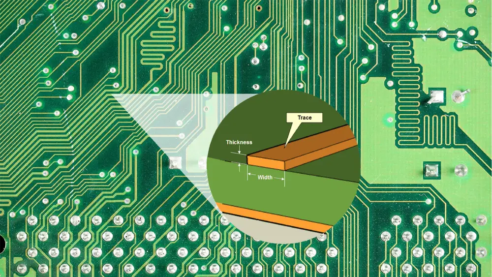
Steps to Measure Voltage. Please turn on the device: First, ensure the PCB or the device it's part of is powered on.It would help if you had electricity flowing through the board to measure the voltage. Set your multimeter: Turn the multimeter dial to the voltage setting.Most digital circuits use DC voltage, so choose that setting.; Connect the probes: Touch the red probe to the positive point Testing a bare PCB involves verifying the integrity of its electrical connections, ensuring that the traces, vias, pads, and layers are fabricated as intended. Without adequate testing at this stage, issues such as open circuits, shorts, and impedance mismatches can go unnoticed, resulting in unreliable or non-functional products down the line.