Digital Frequency Synthesizer Circuit Diagram The synthesizer that we will be designing was extremely common back in the day. It's known as a 1V/Octave synthesizer. This means that for every 1V increase on the input, the output frequency will go up by one octave (i.e., by a factor of 2). Now for this module to work correctly, it needs an exponential converter on the input. Frequency synthesisers form the basis of most radio system designs and their performance is often key to the overall operation. This paper will present an introductory overview of the basic parameters governing the design of a phase locked loop frequency synthesiser and their effects, with the sources of phase noise within a design also being

Analog synthesizers are very cool, but also quite difficult to make. So I wanted to make one as simple as it can get, so its functioning can be easily understandable. For it to work, you need a few basic sub-circuits: A simple oscillator with resistor selectable oscillating frequency, some keys, and a basic amplifier circuit.

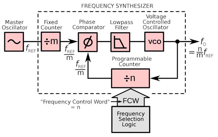
RF Frequency Synthesizer Design: Block Diagram & Components Circuit Diagram
The frequency-divider modulus N have value between 3 to 999 with single steps increment. In locked condition, the comparator and signal are at same frequency that f=N*1kHZ.So we have a frequency synthesizer with 3KHZ to 999 KHZ range with 1-KHZ increment, which can be programed by the switch position of the divide-by-n counter. This circuit
Fractional-N Frequency Synthesizer PFD Charge Pump N sd[m] ref(t) out(t)e(t) div(t) Σ−Δ Modulator v(t) N[m] Loop Filter Divider VCO Focus on this architecture since it is essentially a "super set" of other synthesizers, including integer-N and fractional-N-If we can design and simulate this structure, we can also 11:00 - 12:30 Basic Concepts - Linearity , noise figure, dynamic range 2:00 - 3:30 RF front-end design - LNA, mixer 4:00 - 5:30 Frequency synthesizer design I (PLL) T d J l 22 2008Tuesday, July 22, 2008 9:00 - 10:30 Frequency synthesizer design II (VCO) 11:00 - 12:30 RFIC design for wireless communications The key to turning a timer circuit into a proper wave generator is to realize that its output frequency is a function of the resistances and capacitance of its components. As usual Ben Eater has a terrific explanation of this topic which you can find here. In particular, if we vary the resistance 𝑅 1 R 1 of the circuit, we will vary its

DIY Synth Series Part 1 — The Exponential VCO Circuit Diagram
synthesizer consists of a few standard functions found on a commercial synthesizer. The circuits are constructed with price as a driving consideration. The documentation include a discussion about 5 Design Basics 21 frequency and resonance can often be controlled by a control voltage signal. This can come from