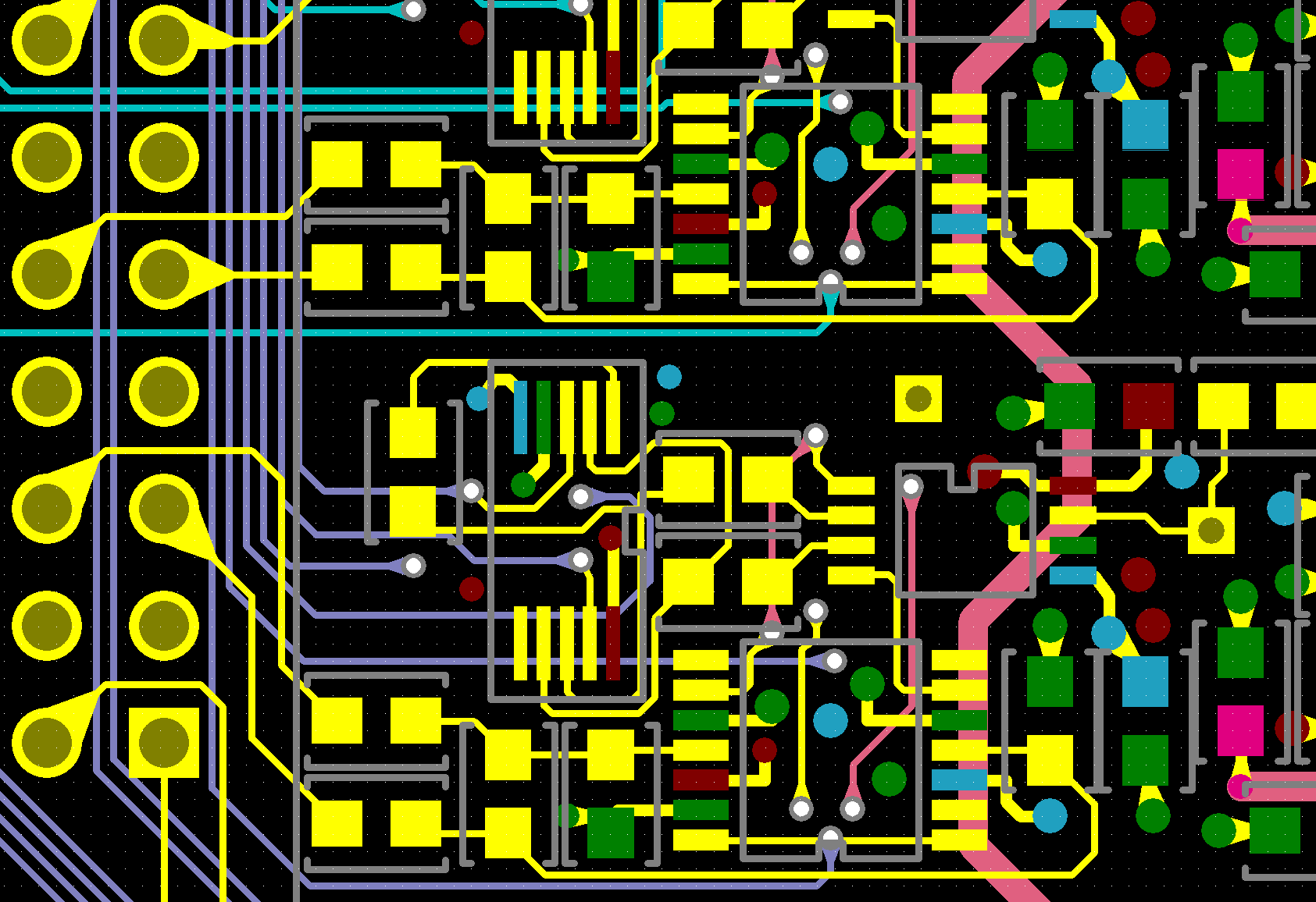
4 steps to review the PCB layout TechnieX Circuit Diagram PCB layout design is a critical skill that directly affects the performance, reliability, and cost of an electronic device. By following best practices such as optimizing component placement, maintaining signal integrity, and ensuring proper thermal management you can create a PCB layout that meets both technical and manufacturing requirements. Step 3: PCB layout stage. The PCB layout stage includes setting up the design tool, board outline, netlist import, component placement, routing, silkscreen cleanup, DRC check, and generating documents for production (Gerbers, netlist, etc.). Setting up the stack-up. The board layout is started by setting the stack-up and design rules.

Step 3: Create PCB layout. Convert schematics into PCB layouts. Select the appropriate PCB size and shape, which takes into account space for mounting, heat dissipation requirements, and fit with other PCBs. Components are shown as footprints with pads and connection lines in the PCB layout. You can see how the components will physically look For beginners, TechSparks recommends initiating the design process with the PCB schematic.The schematic serves as the foundation for circuit design, illustrating the interconnection relationships among electronic components and circuit functions. Guided by the schematic, the designer strategically plans and arranges the placement of electronic components on the PCB. Create Gerber Files in KiCad. From the PCB Editor in KiCad you can create Gerber files by going to the File menu and selecting Plot… A window will appear. Click on the Plot button to create the Gerber files. To create Drill files, click on Generate Drill Files… to open the Drill File dialog. Then click the button Generate Drill File.

How to Design a Printed Circuit Board in 10 Easy Steps Circuit Diagram
Step 2: Create a Blank PCB Layout. After you've created your schematic, for the next PCB design step you'll need to use the schematic capture tool in Altium Designer to import components into a blank PCB layout. First, create a blank printed circuit board document which will generate a PcbDoc file. PCB layout design is the process of arranging electronic components, conductive traces, power planes, and other elements on a circuit board to facilitate the flow of electrical signals and meet the functional requirements of the electronic system. Connect all ground points to the ground plane to create a low impedance return path for

A step-by-step guide to PCB design and layout. Everything you need to know to convert a prototype circuit into a fully optimized PCB. A step-by-step guide to PCB design and layout. When designing a multi-layer PCB, you may need to create links between the various layers of your PCB. You can use a via or a component through hole to achieve that.

The Ultimate Guide to PCB Layout Design Circuit Diagram
Step 4: Get Your PCB Made. When you're finished drawing your PCB design, you need to get the design made. You could etch your PCB at home, but my preferred way is to just order a PCB from one of the many PCB manufacturers out there. Choosing the right PCB design software is crucial to an efficient design process. Some of the most commonly used tools include: Altium Designer: A powerful, feature-rich tool for professional PCB design. KiCAD: An open-source software suitable for beginners and hobbyists. Eagle: Ideal for small to medium-sized projects with a user-friendly